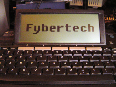
Mailstation Development
The ultimate goal of modding the Mailstation for me has been to run the CP/M operating system and applications written for it. On the one hand, the Mailstation is more than capable of handling this, since it has Flash memory for storage, an LCD for output, a keyboard for input, and more than enough RAM for the OS and applications. On the other hand, however, the default configuration of the Mailstation's address space makes it impossible to actually run the operating system.
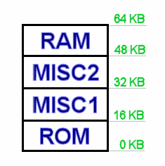
| Mailstation Address Layout: | Necessary for CP/M: |
 |
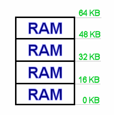 |
CP/M relies on there being RAM in the first 256 bytes of address space for setting system variables, pointers, and buffers. CP/M applications then expect to be loaded at address 0x100, and call OS functions via the RAM configured below.
The Mailstation reserves the first 16KB of address space for ROM. In this "slot" is the first 16KB of the 1MB Flash chip which stores the Mailstation OS. The upper 16KB of address space is reserved for the first 16KB of the 128KB SRAM chip. The middle two slots, labeled "MISC1" and "MISC2" in the above diagram, can actually be switched between the various hardware devices, including the 128KB SRAM, 1MB Code Flash, 512KB Data Flash, the LCD, and the modem. For the RAM and Flash chips, you can set which 16KB page you want to access via each slot, as well. That means the SRAM is broken into 8 pages, the Code Flash into 64 pages, and the Data Flash into 32 pages.
So with a stock Mailstation, you can configure the entire upper 48KB of address space as RAM. Unfortunately, the Code Flash is always in the bottom, and therefore a problem.
This hardware mod lets me switch out the lowest 16KB of address space with the second 16KB page of SRAM. The reason I chose the second is because the first page is always in the upper 16KB of address space, and we wouldn't want to access the same RAM page in two different locations, since that would be a waste of address space.
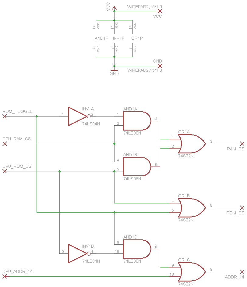
The basic description of this mod is that we've added in a new signal, labeled "ROM_TOGGLE", which changes what device is accessed when read and write operations are attempted on the first 16KB of Code Flash. When this signal is logic high, any attempts to access the first 16KB of Code Flash are redirected to the SRAM instead. Address line 14 is also forced high during access, ensuring that the second page of SRAM is accessed rather than the first.
 (click to enlarge) |
 (click to enlarge) |
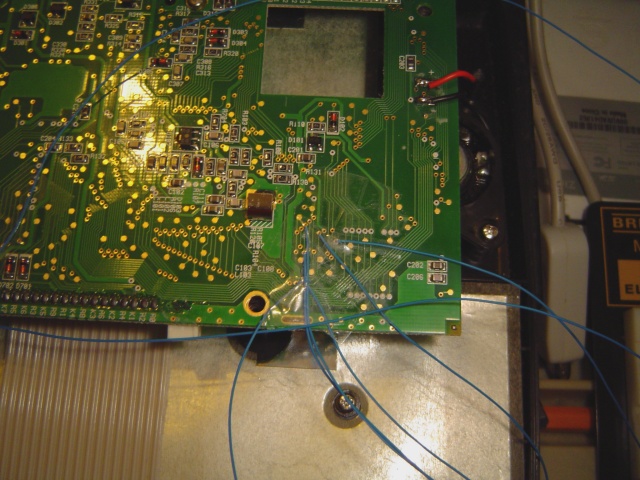
What takes the longest is simply following the traces by eye to find the best location to take advantage of. I used a section on the back of the board, where the signals I wanted conveniently traveled through two eyelets close to each other. So I was able to simply slice the traces between them, then solder wires to the eyelets on either side of the cut. You'll probably want to test continuity between eyelets whenever you cut a trace, because you want to make sure you severed the connection completely!
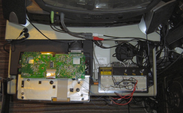
Here are some photos of the approach I took.
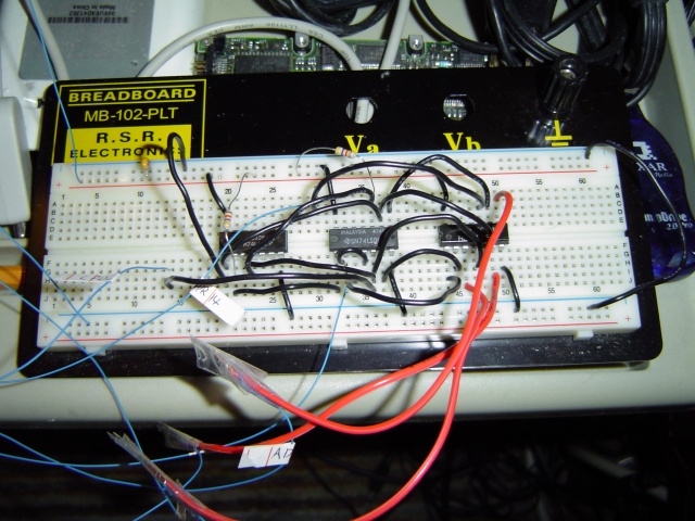
The prototype breadboard version. Not being an electronics expert, I decided it was much smarter to test my design before I go soldering anything. It wasn't pretty, but it worked!
I didn't even solder the wires into the board originally. I used a small-gauge wire, hooked the tips slightly, rested them into the eyelets, and just taped them down.
Notice that I'm tapping into the 5V and ground over closer to the keyboard cable. Where you get your power is up to you.
It was a bit cumbersome to use the Mailstation like this, especially since I still had to be able to transfer code for testing via the parallel port. But I managed! It just needed to work well enough to see if RAM was properly switching into position. At this point, I was still operating the ROM_TOGGLE line manually, too.
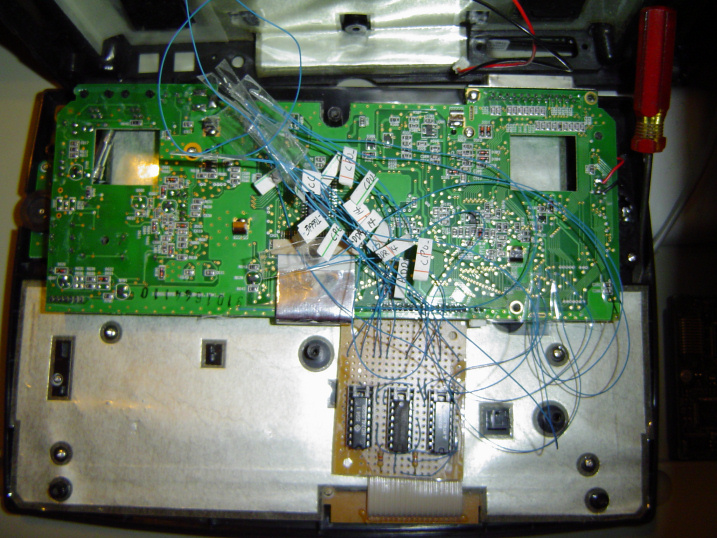
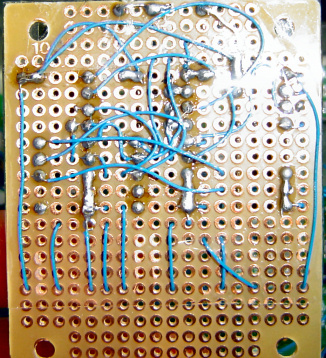
So much wire! This is obviously after I constructed a perf board version, once I was sure it worked okay. I left a lot of slack wire on the board, and soldered separate wires into the Mailstation itself. I wanted the board to still be "modular" in case I needed to make any changes to it at some point. I didn't have any connectors laying around, so I just twisted and taped the wire ends together. Not pretty, and leaves lots of slack wire, but at least it works.
Something very important, if you ask me, is that you label every wire. I labeled the ones coming from the Mailstation board as well as the ones on the add-on board. That way I definitely wouldn't make any mistakes when wiring it together!
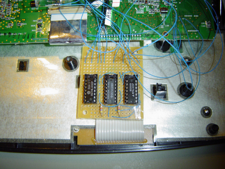
Not an expert at soldering! It was the first real board I ever assembled, though, so it came out better than I expected.
So, even when you have this capability to toggle the RAM and ROM, you might be wondering HOW you actually toggle it. If you want to use the same method I used, then you can connect ROM_TOGGLE to I/O port 28, bit 3 (CPU pin 81). Now, keep in mind, on my DET1, this signal was available for me to tap into. However, I'm not sure if other model Mailstations might actually use this for caller ID or something. I've never messed with any of the other models, so I simply can't tell you what's connected to that pin on those (if anything).
When the Mailstation powers up, port 28 is set as an input. So my ROM_TOGGLE line ended up pulling itself high, and therefore never booting (since it was running from uninitialized RAM). So I put a 1K pull-down resistor on it, which forces it low unless P28 is configured as output and is "high".
To toggle RAM into place, first you set port 28.3 as an output via port 29. Then you simply enable bit P28.3. If all is well, any future accesses to Code Flash 0x0000-0x3FFF should go to RAM 0x4000-0x7FFF.
If you want to take the mod one step further, you can add a switch between a pull-up and ROM_TOGGLE too. This would allow you to force RAM into place at Mailstation startup. This can be useful if you want to test code that you might eventually write into the Code Flash, but don't want to risk bricking your Mailstation without testing it first (especially from an uninitialized hardware state). What you would do is start up normally, write your code into RAM, flip your switch to force ROM_TOGGLE high, then power down/reset the Mailstation. As long as you never remove the batteries or AC adapter, the RAM contents are saved, meaning whatever you wrote should still be there at next power up, which is what it will boot from. Where you physically put your switch to force ROM_TOGGLE is up to you. I put mine in the battery compartment.